
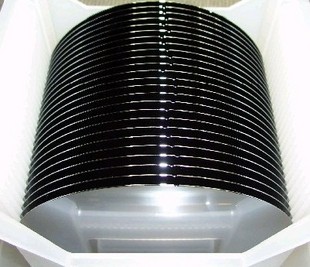
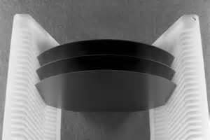
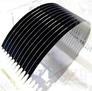
CZ silicon wafers
WaferHome can manufacture the high purity 99.999999999% IC grade silicon wafer
Contact info
E-mail waferhome@hotmail.comSpecification for CZ Growth Siliocn Wafer
| Grade | Dimeter | Type/dopant | Orientaion | thickness | Resistivity | Flat |
Surface/Roughness | Geometric parameter |
|---|---|---|---|---|---|---|---|---|
| Prime | 25.4mm 50.8mm 76.5mm | P(Boron) N(Phos/As/Sb) | <100> <111> or special orientation |
400um+/-20 400um+/- 20 400um+/-20 | 0.0001 - 200 Ohm-cm /Customization |
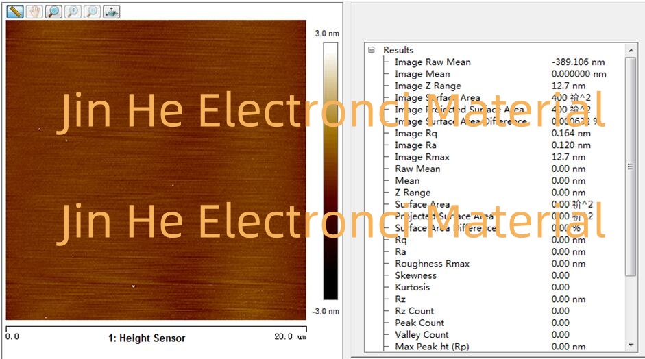
N/A 16mm 22.5mm | polished/etched polished/polished | TTV < 5um TIR <3um STIR < 2um BOW < 20um Warp < 30um Ra<0.5nm |
| 100mm 125mm 150mm | P(Boron) N(Phos/As/Sb) | <100> <111> or special orientation | 525um+/-20 625um+/-20 625um+/-20 | 0.0001 - 200 Ohm-cm /Customization | 32.5mm 42.5mm 57.5mm | polished/etched polished/polished | TTV < 5um TIR <3um STIR < 2um BOW < 20um Warp < 30um Ra<0.5nm | |
| 200mm | P(Boron) N(Phos/As/Sb) | <100> <111> or special orientation | 725um+/-20 | 0.0001 - 200 Ohm-cm /Customization | nothch/flat | polished/etched polished/polished | TTV < 5um TIR <3um STIR < 2um BOW < 20um Warp < 30um Ra<0.5nm | |
| 300mm | P(Boron) N(Phos/As/Sb) | <100> <111> or special orientation | 775um+/-20 | 0.0001 - 200 Ohm-cm /Customization | notch/flat | polished/etched polished/polished | TTV < 5um TIR <3um STIR < 2um BOW < 20um Warp < 30um Ra<0.5nm | |
| Dummy | 25.4mm 50.8mm 76.5mm | P(Boron) N(Phos/As/Sb) | <100> <111> or special orientation |
400um+/-20 400um+/- 20 400um+/-20 | 0.0001 - 200 Ohm-cm /Customization |
N/A 16mm 22.5mm | polished/etched polished/polished | TTV < 5um TIR <3um STIR < 2um BOW < 20um Warp < 30um Ra<0.5nm |
| 100mm 125mm 150mm | P(Boron) N(Phos/As/Sb) | <100> <111> or special orientation | 525um+/-20 625um+/-20 625um+/-20 | 0.0001 - 200 Ohm-cm /Customization | 32.5mm 42.5mm 57.5mm | polished/etched polished/polished | TTV < 5um TIR <3um STIR < 2um BOW < 20um Warp < 30um Ra<0.5nm | |
| 200mm | P(Boron) N(Phos/As/Sb) | <100> <111> or special orientation | 725um+/-20 | 0.0001 - 200 Ohm-cm /Customization | nothch/flat | polished/etched polished/polished | TTV < 5um TIR <3um STIR < 2um BOW < 20um Warp < 30um Ra<0.5nm | |
| 300mm | P(Boron) N(Phos/As/Sb) | <100> <111> or special orientation | 775um+/-20 | 0.0001 - 200 Ohm-cm /Customization | notch/flat | polished/etched polished/polished | TTV < 5um TIR <3um STIR < 2um BOW < 20um Warp < 30um Ra<0.5nm | |
| extra thick wafer | 25.4mm 50.8mm 76.5mm | P(Boron) N(Phos/As/Sb) | <100> <111> or special orientation |
>=1000um customization | 0.0001 - 200 Ohm-cm /Customization |
N/A 16mm 22.5mm | polished/etched polished/polished | TTV < 5um TIR <3um STIR < 2um BOW < 20um Warp < 30um Ra<0.5nm |
| 100mm 125mm 150mm | P(Boron) N(Phos/As/Sb) | <100> <111> or special orientation | >=1000um customization | 0.0001 - 200 Ohm-cm /Customization | 32.5mm 42.5mm 57.5mm | polished/etched polished/polished | TTV < 5um TIR <3um STIR < 2um BOW < 20um Warp < 30um Ra<0.5nm | |
| 200mm | P(Boron) N(Phos/As/Sb) | <100> <111> or special orientation | >=1000um customization | 0.0001 - 200 Ohm-cm /Customization | notch/flat | polished/etched polished/polished | TTV < 5um TIR <3um STIR < 2um BOW < 20um Warp < 30um Ra<0.5nm | |
| 300mm | P(Boron) N(Phos/As/Sb) | <100> <111> or special orientation | >=1000um customization | 0.0001 - 200 Ohm-cm /Customization | notch/flat | polished/etched polished/polished | TTV < 5um TIR <3um STIR < 2um BOW < 20um Warp < 30um | |
| extra thin wafer | 25.4mm 50.8mm 76.5mm | P(Boron) N(Phos/As/Sb) | <100> <111> or special orientation |
100um 200um customization | 0.0001 - 200 Ohm-cm /Customization |
N/A 16mm 22.5mm | polished/etched polished/polished | TTV < 5um TIR <3um STIR < 2um BOW < 20um Warp < 30um Ra<0.5nm |
| 100mm 125mm 150mm | P(Boron) N(Phos/As/Sb) | <100> <111> or special orientation | 1000um 2000um customization | 0.0001 - 200 Ohm-cm /Customization | 16mm+/-2mm | polished/etched polished/polished | TTV < 5um TIR <3um STIR < 2um BOW < 20um Warp < 30um Ra<0.5nm | |
| 200mm | P(Boron) N(Phos/As/Sb) | <100> <111> or special orientation | 1000um 2000um customization | 0.0001 - 200 Ohm-cm /Customization | 16mm+/-2mm | polished/etched polished/polished | TTV < 5um TIR <3um STIR < 2um BOW < 20um Warp < 30um Ra<0.5nm | |
| 300mm | P(Boron) N(Phos/As/Sb) | <100> <111> or special orientation | 1000um 2000um customization | 0.0001 - 200 Ohm-cm /Customization | 16mm+/-2mm | polished/etched polished/polished | TTV < 5um TIR <3um STIR < 2um BOW < 20um Warp < 30um Ra<0.5nm | |
| extra flat wafer | 25.4mm 50.8mm 76.5mm | P(Boron) N(Phos/As/Sb) | <100> <111> or special orientation |
400um+/-20 400um+/- 20 400um+/-20 | 0.0001 - 200 Ohm-cm /Customization |
N/A 16mm 22.5mm | polished/etched polished/polished | TTV < 2um TIR <1um STIR < 1um BOW < 10um Warp < 10um Ra<0.5nm |
| 100mm 125mm 150mm | P(Boron) N(Phos/As/Sb) | <100> <111> or special orientation | 525um+/-20 625um+/-20 625um+/-20 | 0.0001 - 200 Ohm-cm /Customization | 32.5mm 42.5mm 57.5mm | polished/etched polished/polished | TTV < 2um TIR <1um STIR < 1um BOW < 10um Warp < 10um Ra<0.5nm | |
| 200mm | P(Boron) N(Phos/As/Sb) | <100> <111> or special orientation | 725um+/-20 | 0.0001 - 200 Ohm-cm /Customization | nothch/flat | polished/etched polished/polished | TTV < 2um TIR <1um STIR < 1um BOW < 10um Warp < 10um Ra<0.5nm | |
| 300mm | P(Boron) N(Phos/As/Sb) | <100> <111> or special orientation | 775um+/-20 | 0.0001 - 200 Ohm-cm /Customization | notch/flat | polished/etched polished/polished | TTV < 2um TIR <1um STIR < 1um BOW < 10um Warp < 10um Ra<0.5nm |